
VM-AI1i Assembly step by step
This page show how to correctly assembly the VM-AI1i kit (elaboration unit), step by step.
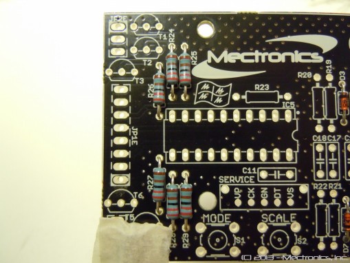
The PCBs
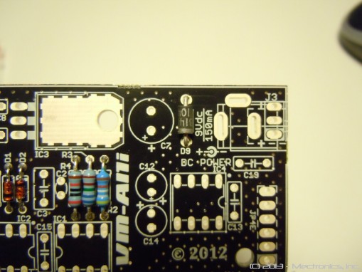
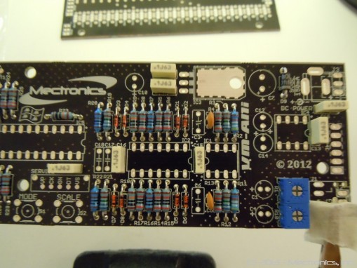
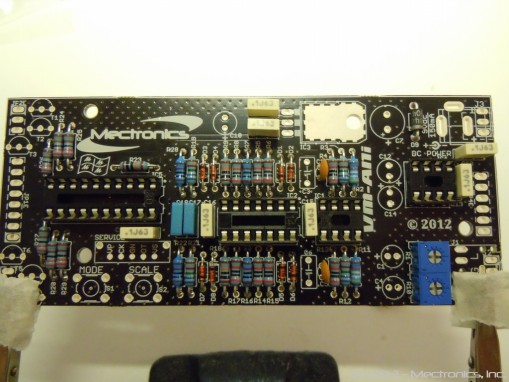
Figure 1 shown the two PCBs that are the mechanical support of VM-AI1i. As you can see, are two-layer PCBs, with double side ground plane and star ground (elaboration unit). A state-of-art PCBs, obviously Made in Italy!
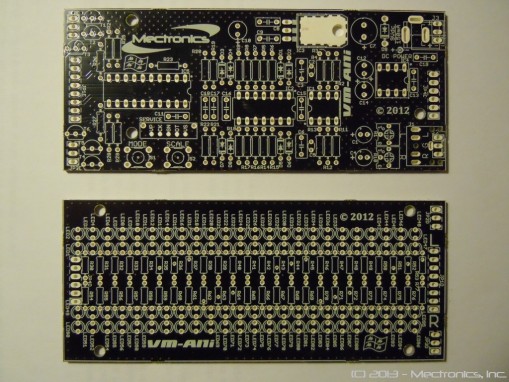
VM-AI1i – The PCBs
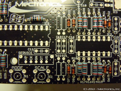
The kit parts
Figure 2 shown the parts that compose the VM-AI1i kit. All components are first class, only the best of the best: metal-film 1% resistor from Vishay, audio grade and low-esr electrolytic capacitors from Nichicon and Kemet, film capacitors from Wima and Panasonic, Op-Amp from Texas Instruments, MCU from Microchip, leds from Avago and Kingbrite, mechanical (header, sockets) parts from 3M etc etc…
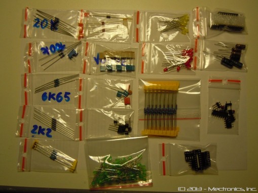
VM-AI1i – The Parts
Bill of Material
Below there is the bill of material of the elaboration unit of VM-AI1i kit.
Resistors
| Name | Value | Notes/Color code |
|---|---|---|
| R1, R10 (2X) | 50kΩ | 1/4in Trimmer |
| R2, R11 (2X) | 49.9 kΩ, ¼ W, ±1% | Yellow White White Red Brown |
| R3, R12, R19, R21 (4X) | 6.65 kΩ, ¼ W, ±1% | Blue Blue Green Brown Brown |
| R4, R5, R6, R8, R13, R14, R15, R17 (8X) | 20 kΩ, ¼ W, ±1% | Red Black Black Red Brown |
| R7, R16 (2X) | 10 kΩ, ¼ W, ±1% | Brown Black Black Red Brown |
| R9, R18, R23 (3X) | 100 kΩ, ¼ W, ±1% | Brown Black Black Orange Brown |
| R20, R22 (2X) | 1 kΩ, ¼ W, ±1% | Brown Black Black Brown Brown |
| R24…R29 (6X) | 2.2 kΩ, ¼ W, ±1% | Red Red Black Brown Brown |
Capacitors
| Name | Value | Notes |
|---|---|---|
| C1, C4 (2X) | 1uF, 50V | Electrolytic, Audio Grade |
| C2, C5 (2X) | 120pF | Ceramic |
| C3, C6 (2X) | 1uF, 50V | Polyester film |
| C7 (1X) | 470uF, 25V | Electrolytic |
| C8, C9, C11, C13, C15, C16, C19 (7X) | 100nF, 63V | Polyester film |
| C10 (1X) | 10uF, 25V | Electrolytic |
| C12, C14 (2X) | 100uF, 25V | Low-ESR Electrolytic |
| C17, C18 (2X) | 220nF, 63V | Polyester film |
Discrete Semiconductors
| Name | Value | Notes |
|---|---|---|
| D1…D8 (8X) | 1N4148 | Switching diode |
| D9 (1X) | SB140 | Schottky barrel diode |
| T1…T6 (6X) | BC337 | NPN g.p. transistor |
Integrated semiconductors
| Name | Value | Notes |
|---|---|---|
| IC1 (1X) | TC1044S | Charge pump |
| IC2 (1X) | TL072 | Dual low-noise operational amplifier |
| IC3 (1X) | LM7805 | 5V Voltage regulator |
| IC4 (1X) | TL074 | Quad low-noise operational amplifier |
| IC5 (1X) | – | VM-AI1i v3.5/2013 Preprogrammed MCU |
Mechanical/spare parts
| Name | Value | Notes |
|---|---|---|
| JP1E (1X) | 8 Pin Male header | |
| JP2E, JP3E (2X) | 3 Pin Male header | |
| JP4E (1X) | 6 Pin Male header | |
| S1, S2 (2X) | N.O. Tactile buttons | |
| 2X 8Pin 2.54mm/0.1in IC socket | ||
| 1X 14Pin2.54mm/0.1in IC socket | ||
| 1X 20Pin 2.54mm/0.1in IC socket | ||
| JP1D (1X)* | 8 Pin Female header | |
| JP2D, JP3D (2X) | 3 Pin Female header | |
| JP4D (1X) | 6 Pin Female header |
* In italics there are the display units mechanical parts.
Ok, let’s go to start!
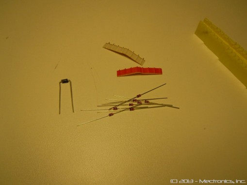
Step #1
Bend the resistors (ALL resistor; the picture show how done this step using a bending tool).

VM-AI1i-AssemblyStep01
Step #2
Separates the diodes.

VM-AI1i-AssemblyStep02
Step #3
Bend the diodes.
VM-AI1i-AssemblyStep03
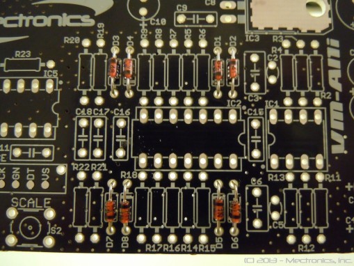
Step #4
Solder the eight 1N4148 (D1…D8) diodes. Notes the direction Anode-Cathode (the side with the black band painted).
VM-AI1i-AssemblyStep04
Step #5
Solder the six 2.2k (R24…R29) resistors.
VM-AI1i-AssemblyStep05
Step #6
Solder the two 49.9k (R2, R11) resistors.

VM-AI1i-AssemblyStep06
Step #7
Solder the eight 20k (R4…R6, R8, R13…R15, R17) resistors.

VM-AI1i-AssemblyStep07
Step #8
Solder the three 100k (R9, R18, R23) resistors.
VM-AI1i-AssemblyStep08
Step #9
Solder the four 6.65k (R3, R12, R19, R21) resistor.
VM-AI1i-AssemblyStep09
Step #10
Solder the two 1k (R20, R22) resistor.
VM-AI1i-AssemblyStep10
Step #11
Solder the two 10k (R7, R16) resistor.

VM-AI1i-AssemblyStep11
Step #12
Solder the SB140A (D9) Schottky diode.
VM-AI1i-AssemblyStep12
Step #13
Solder the two 50k (R1, R10) trimmers, the two 120pF (C2, C5) ceramic capacitors and the seven 100nF (C8, C9, C11, C13, C15, C16, C19) film capacitors.
VM-AI1i-AssemblyStep13
Step #14
Solder the two 220nF (C17, C18) film capacitors and the four sockets (two 8P, one 14P and one 20P), looking carefully the references.
VM-AI1i-AssemblyStep14
Step #15
Solder the two buttons (S1, S2).

VM-AI1i-AssemblyStep15
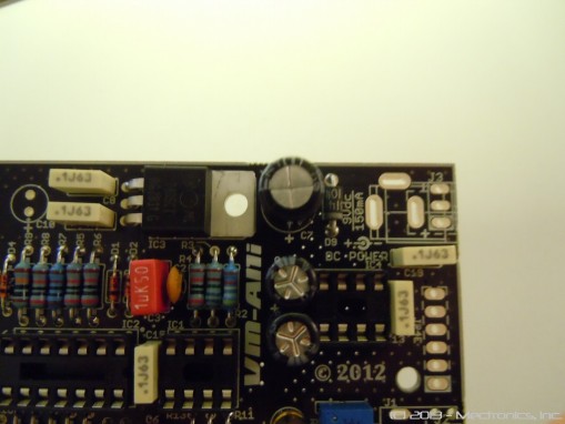
Step #16
Using a nail, bend the pins of uA7805 regulator…
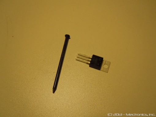
VM-AI1i-AssemblyStep16
Step #17
…in this way!

VM-AI1i-AssemblyStep17
Step #18
Solder the uA7805 (IC3) voltage regulator.
VM-AI1i-AssemblyStep18
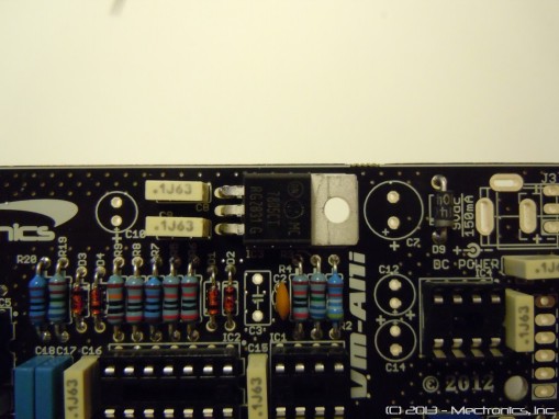
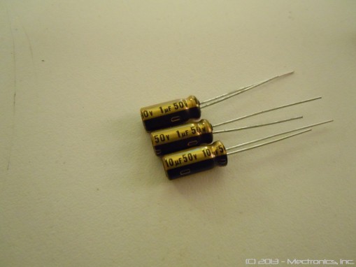
Step #19
Look carefully this capacitors: there are two 1uF/50V capacitors and only one 10uF/50V.
VM-AI1i-AssemblyStep19
Step #20
Solder the 10uF/50V (C10) capacitor.

VM-AI1i-AssemblyStep20
Step #21
Solder the two 100uF/25V (C12, C14) Low-esr capacitors and the two 1uF/50V (C3, C6) film capacitors.
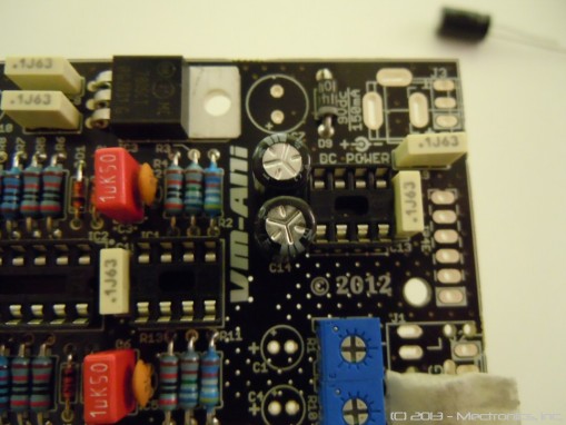
VM-AI1i-AssemblyStep21
Step #22
Solder the two 1uF/50V (C1, C4) audio grade capacitors.

VM-AI1i-AssemblyStep22
Step #23
Solder the 470uF/25V (C7) filter capacitor.
VM-AI1i-AssemblyStep23
Step #24
Join the headers with the sockets.
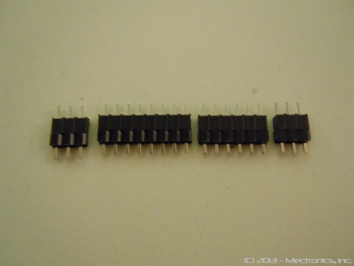
VM-AI1i-AssemblyStep24
Step #25
Finally, solder the headers. After, using a flux cleaner, we can remove the excess flux.
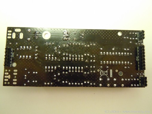
VM-AI1i-AssemblyStep25
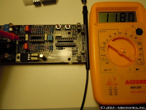
Step #26
Ok, now we can measure the voltages (I’ve used a 12Vdc power supply source). Point #1 – Cathode of D9, expected value: 11.8V.

VM-AI1i-AssemblyStep26
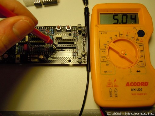
Step #27
Voltage measuring. Point #2 – out of IC3, expected value: 5V.
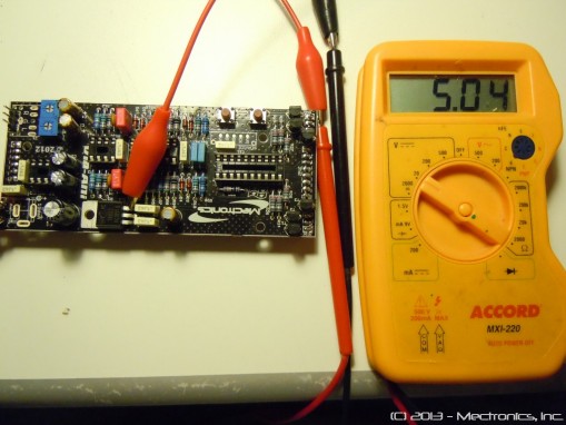
VM-AI1i-AssemblyStep27
Step #28
The linear ICs. There are one charge pump (IC4, TC1044SCPA) voltage converter, one dual-low-noise (IC1, TL072) operational amplifiers and one quad-low-noise (IC2, TL074) operational amplifiers.
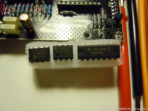
VM-AI1i-AssemblyStep28
Step #29
Insert the charge pump IC (IC4, TC1044SCPA) . Look carefully the reference (pin #1).

VM-AI1i-AssemblyStep29
Step #30
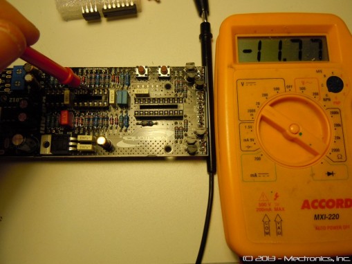
Voltage measuring. Point #3 – pin #4 of IC1, expected value: -11.8V.

VM-AI1i-AssemblyStep30
Step #31
Voltage measuring. Point #4 – pin #11 of IC2, expected value: -11.8V.
VM-AI1i-AssemblyStep31
Step #32
Voltage measuring. Point #5 – pin #1 of IC4, expected value: 5V.
VM-AI1i-AssemblyStep32
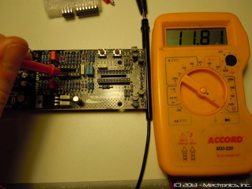
Step #33
Voltage measuring. Point #6 – pin #8 of IC1, expected value: 11.8V.
VM-AI1i-AssemblyStep33
Step #34
Voltage measuring. Point #7 – pin #4 of IC2, expected value: 11.8V.
VM-AI1i-AssemblyStep34
Step #35
Ok, after correctly inserting the linear integrated circuits and the preprogrammed MCU, the heart of VM-AI1i, we are ready to the final test (I’ve used the old display).
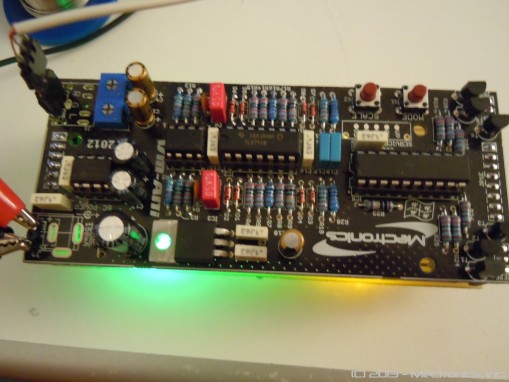
VM-AI1i-AssemblyStep35
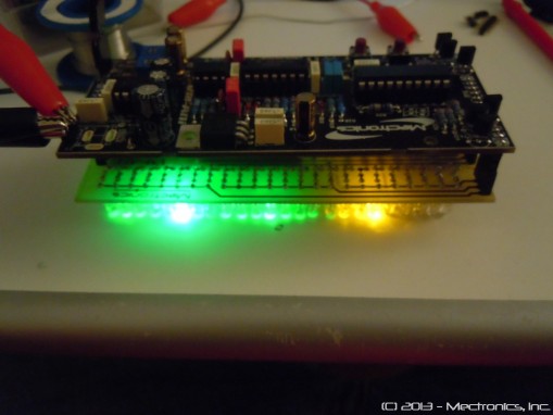
Step #36
…and that’s it! Enjoy!
VM-AI1i-AssemblyStep36